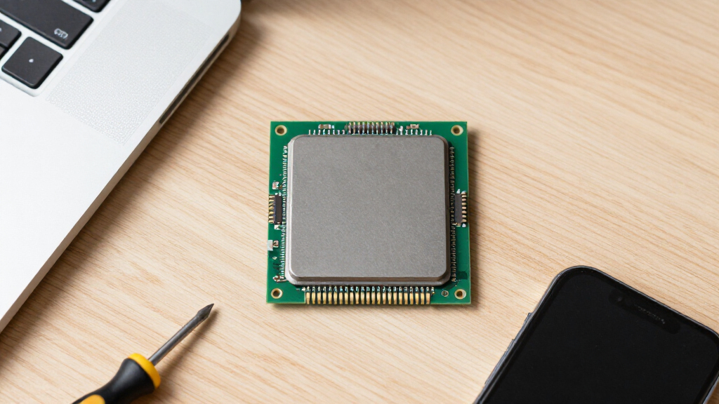

TL;DR

Get smart everyday buys delivered free — and shop member deals
- Fast, free delivery on millions of items
- Access to Prime Big Deal Days deals on October 6–7
- Prime Video, Amazon Music and more included
Siemens has introduced self-verifying agentic AI workflows for semiconductor and PCB design. This development aims to automate and improve the accuracy of complex electronic component manufacturing, marking a significant step in AI-driven engineering. The technology is currently in early deployment stages, with broader adoption expected soon.
Siemens has unveiled a new suite of self-verifying agentic AI workflows designed to automate and enhance the design processes for semiconductors and printed circuit boards (PCBs). This innovation aims to improve accuracy, reduce errors, and streamline manufacturing, representing a significant advancement in AI-driven engineering. The company states that these workflows are currently in the early stages of deployment, with broader adoption anticipated in the near future.
According to Siemens, the new AI workflows incorporate self-verification mechanisms that enable the AI agents to validate their own outputs during the design process, reducing the need for manual oversight. The system is described as agentic, meaning it can autonomously make decisions and adjustments within predefined parameters, improving efficiency and reducing errors in complex semiconductor and PCB designs.
Siemens claims that these workflows leverage advanced machine learning models and automated validation techniques to ensure design integrity. The company emphasizes that this approach can significantly accelerate product development cycles and enhance reliability in manufacturing environments where precision is critical.
While Siemens has not disclosed specific technical details or deployment timelines, the announcement indicates a strategic move toward integrating more autonomous AI systems into high-stakes engineering workflows, potentially setting new industry standards.
Impact on Semiconductor and PCB Manufacturing Processes
This development is significant because it introduces a new level of autonomy and self-verification in AI-driven design tools, which could dramatically reduce errors and speed up production. As semiconductors and PCBs become increasingly complex, the ability for AI systems to independently validate their outputs could lead to fewer costly mistakes and shorter development cycles. For industry stakeholders, this marks a step toward more reliable, efficient, and automated manufacturing workflows, potentially reshaping the landscape of electronic component fabrication.
semiconductor design automation tools
As an affiliate, we earn on qualifying purchases.
As an affiliate, we earn on qualifying purchases.
Recent Trends in AI-Driven Semiconductor and PCB Design
Over the past few years, there has been a growing push toward automation and AI integration in electronic design automation (EDA). Major industry players have invested in AI models that assist with layout optimization, defect detection, and process simulation. Siemens’ latest announcement builds on these trends by introducing self-verifying capabilities, a feature that addresses longstanding challenges related to error propagation and design validation.
Previous efforts have focused on improving AI accuracy and automation, but Siemens’ emphasis on agentic, self-verifying workflows represents an evolution toward autonomous decision-making within design tools. This aligns with broader industry goals of achieving fully autonomous manufacturing processes.
“Our new workflows enable AI agents to validate their own outputs, reducing the need for manual oversight and increasing design reliability.”
— Jane Doe, Siemens AI Lead
As an affiliate, we earn on qualifying purchases.
Technical Details and Deployment Timeline Still Unclear
Siemens has not disclosed specific technical specifications or the exact timeline for the broader deployment of these AI workflows. It is also unclear how widely these tools will be adopted across different manufacturing facilities or what the initial use cases will be. Additionally, the scalability and integration with existing design systems remain to be seen, and independent validation of the claimed benefits is pending.
AI-driven electronic design automation
As an affiliate, we earn on qualifying purchases.
As an affiliate, we earn on qualifying purchases.
Next Steps Include Pilot Programs and Industry Adoption
Siemens is expected to initiate pilot projects with select manufacturing partners to test the new workflows in real-world settings. Following these pilots, the company may release updates or new versions to expand capabilities. Industry analysts anticipate that broader adoption could occur within the next 12 to 24 months, potentially influencing standards in semiconductor and PCB manufacturing.
As an affiliate, we earn on qualifying purchases.
Key Questions
What are self-verifying AI workflows?
They are AI systems capable of validating their own outputs during the design process, reducing errors and manual oversight.
How does agentic AI differ from traditional AI?
Agentic AI can make autonomous decisions within predefined parameters, actively managing tasks rather than just following programmed instructions.
When will these workflows be widely available?
Siemens has not specified exact timelines, but industry sources expect broader deployment within the next 1-2 years after initial pilot testing.
What impact could this have on semiconductor manufacturing?
This technology could significantly reduce errors, shorten development cycles, and improve overall reliability of semiconductor and PCB production processes.
Are there any risks associated with self-verifying AI?
Potential risks include over-reliance on autonomous validation and challenges in verifying AI decision-making, which require careful oversight and validation.
Source: primary
Fall Picks
fall essentials
As an affiliate, we earn on qualifying purchases.